

-
PAPER
3D Integrated Process and Hybrid Bonding of High Bandwidth Memory (HBM)

 관리자2025-05-01 조회 291 댓글 0
이메일주소 site@site.co.kr Author Chae Yeon Lee, Chae Ho Won, Seyeon Jung, Eun Su Jung, Tae Min Choi, Hwa Rim Lee, JinUk Yoo, Songhun Yoon, Sung Gyu Pyo Journal Electronic Materials Letters Year of Pub. 2025 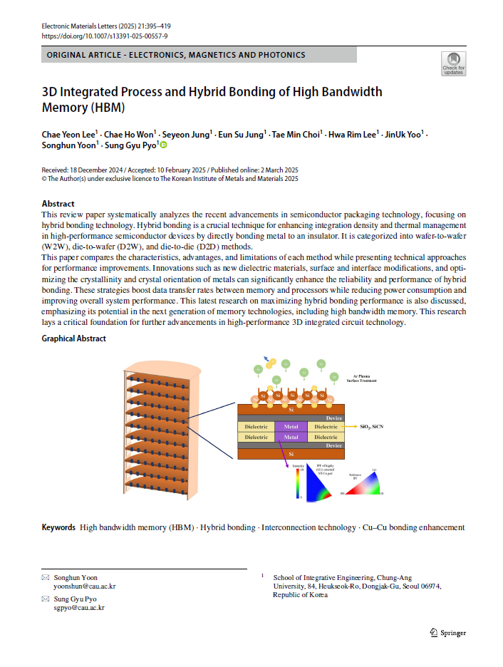
3D Integrated Process and Hybrid Bonding of High Bandwidth Memory (HBM)
This review paper systematically analyzes the recent advancements in semiconductor packaging technology, focusing on hybrid bonding technology. Hybrid bonding is a crucial technique for enhancing integration density and thermal management in high-performance semiconductor devices by directly bonding metal to an insulator. It is categorized into wafer-to-wafer (W2W), die-to-wafer (D2W), and die-to-die (D2D) methods.This paper compares the characteristics, advantages, and limitations of each method while presenting technical approaches for performance improvements. Innovations such as new dielectric materials, surface and interface modifications, and optimizing the crystallinity and crystal orientation of metals can significantly enhance the reliability and performance of hybrid bonding. These strategies boost data transfer rates between memory and processors while reducing power consumption and improving overall system performance. This latest research on maximizing hybrid bonding performance is also discussed, emphasizing its potential in the next generation of memory technologies, including high bandwidth memory. This research lays a critical foundation for further advancements in high-performance 3D integrated circuit technology.
첨부파일 화면_캡처_2025-05-01_145448.png (207.75KB) [0] 2025-05-01 14:55:03


221 HEUK SEOK-DONG, DONGJAK-GU, SEOUL, KOREA TEL: +82-2-820-5769 FAX: +82-2-814-2651 COPYRIGHT©2013 BY NEL. All Rights Reserved.